MAIN ARTICLE
A traditional assembly site becomes an HBM center
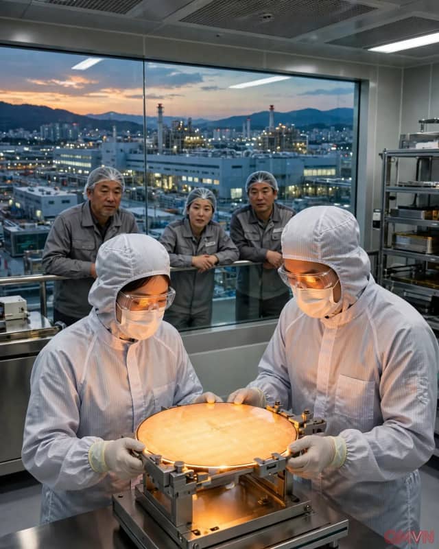
Onyang has long been associated with conventional semiconductor assembly and testing. Samsung now wants to turn it into a center for high-bandwidth memory, or HBM, which vertically stacks DRAM layers to move data rapidly into AI accelerators. Manufacturing the memory dies is only one part of the challenge: layer connections, heat management, power use and final yields determine whether a package can meet demanding customers' specifications.
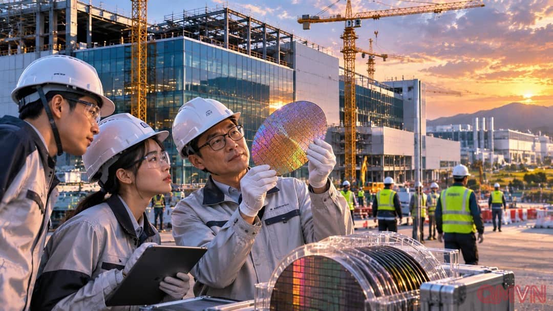
According to Yonhap, Samsung envisages five HBM lines at Onyang. The newest is planned as a three-story building with roughly 31,000 square meters of cleanroom space. The campus's total floor area is expected to rise to about 420,000 square meters from approximately 270,000. These figures describe intended capacity and footprint, not completed production already in service.
Why 46 trillion won is not a single immediate outlay
At the ceremony, President Lee identified 6 trillion won for the advanced packaging factory and an additional 40 trillion won for equipment to be invested in stages. Construction spending and manufacturing equipment should therefore be understood separately.
June 2028 is Samsung's current target for starting the new line, while actual delivery will depend on construction, qualification, equipment availability and market conditions.
Samsung has brought forward the schedule for Line 5 by around one year. In AI infrastructure, bottlenecks extend beyond designing processors to securing reliable packages of high-performance memory at sufficient scale. The early schedule and large budget signal ambition, but neither guarantees market share or profit if yields, pricing or demand evolve unfavorably.
A national megaproject with a regional purpose
The Onyang work forms part of South Korea's flagship industrial program announced in late June, followed by corporate investment pledges in July. Its broad priorities cover semiconductors, AI data centers and physical AI. The Chungcheong groundbreaking also encompasses an advanced display line in Asan and a high-performance substrate manufacturing facility for AI servers in Sejong.
The Korea Herald reported that Samsung, SK Hynix and other companies had pledged around 392 trillion won for the wider Chungcheong region. President Lee also cited an additional 23.6 trillion won planned by 112 companies. Those are regional packages of announcements, not investment solely in the Onyang plant. Adding them to Samsung's 46 trillion won headline figure would misleadingly merge overlapping or differently scoped commitments.
Local benefits must be measured, not presumed
Officials in South Chungcheong Province and Asan were credited with shortening permit procedures to roughly a third of their usual length. The national government promised coordination on power, water and other infrastructure, all crucial to cleanroom-heavy manufacturing. Samsung expects faster implementation to encourage suppliers of materials, components and production equipment to invest as well.
A representative of supplier Daeduck Electronics said 194 specialist businesses aim to invest 18.1 trillion won by 2030, including 66 Chungcheong companies investing or preparing 4.4 trillion won. Job creation numbers remain projections rather than realized outcomes. Policymakers will also need to address housing, transport, technical training and opportunities for smaller companies if the benefits are to be broadly shared.