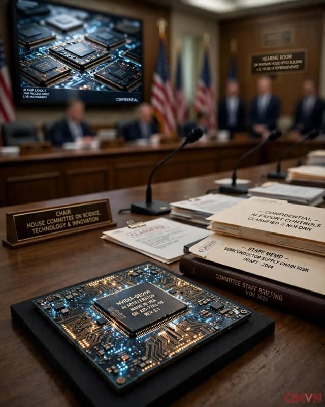
A new line at 16 nanometres
According to the sources, TSMC has instructed that affected orders using manufacturing processes of 16 nanometres and below be halted unless customers obtain US export licences. TSMC guidance reviewed by the two people shows that Chinese designers will generally be limited to 28-nanometre and 40-nanometre processes, provided their chips do not use high-bandwidth memory (HBM) or advanced packaging.
To understand the impact, it helps to look at three key technological elements of AI chips:
- Most leading AI chips are produced on 7-nanometre processes or smaller, enabling faster and more energy-efficient performance.
- HBM allows processors to handle the vast data volumes required by AI applications.
- Advanced packaging integrates chips and memory to boost computing power.
Washington closes the manufacturing route
Previously, TSMC could check the computing power and other technical characteristics of certain Chinese chip designs to determine whether they fell outside US export controls. Under the new rules, which took effect on Thursday, that verification process no longer applies to affected Chinese customers.