MAIN ARTICLE
What the new restrictions mean for orders
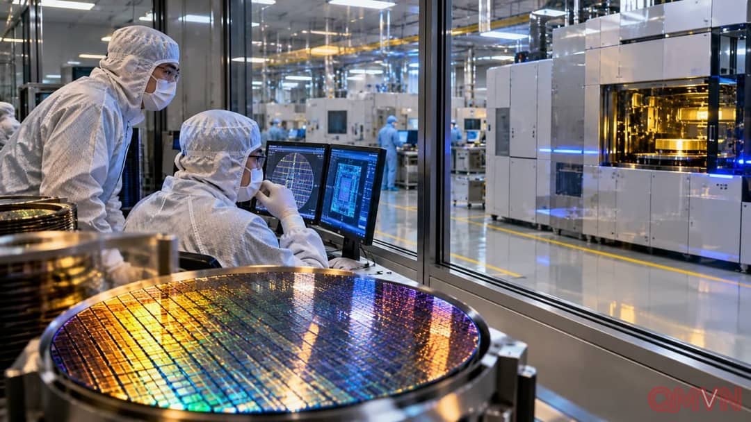
Two people familiar with the situation told Reuters that TSMC had directed affected orders using 16-nanometre and smaller manufacturing processes to stop pending appropriate licensing. That is a report about specific internal guidance, not confirmation that every Chinese customer or every type of semiconductor order has been prohibited.
According to the reported guidance, the affected designers would generally be restricted to established 28- or 40-nanometre production, provided their chips do not incorporate high-bandwidth memory, known as HBM, or require advanced packaging. Those technologies are essential to leading AI accelerators, which must move immense quantities of data between computing units and memory.
In its response to Reuters on November 20, TSMC said it understood and would follow applicable US Bureau of Industry and Security regulations. It also said it does not comment on market rumours. Its official statement should therefore not be confused with independent confirmation of every reported order-level restriction.
Why closing a verification route matters
Previously, TSMC could in certain circumstances examine a proposed chip’s computing performance and other technical attributes to decide whether it fell outside US controls. The new rules narrow that route for affected designers, making a licence or an expressly available exception more important than an individual foundry assessment.