CONTENT
High-density NAND facility upgrades at Xian and Dalian production hubs
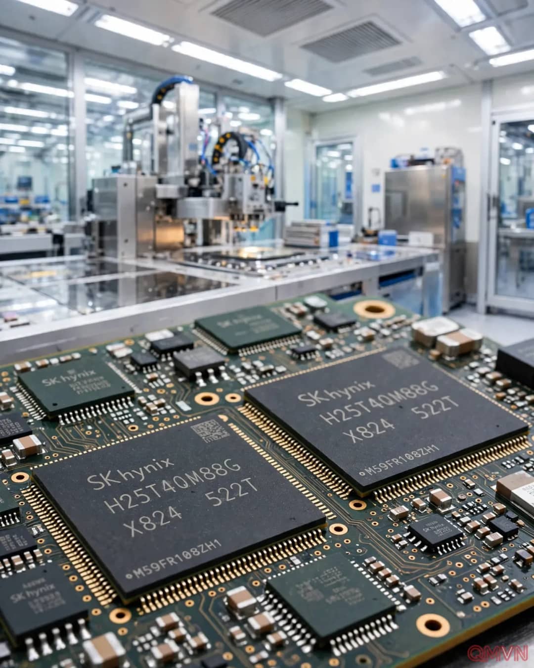
To defend their global competitive standing against surging domestic rivals and fulfill booming demand for artificial intelligence storage solutions, Samsung Electronics and SK Hynix are actively retrofitting their Chinese fabrication facilities to handle cutting-edge NAND flash architectures. Samsung's flagship manufacturing complex in Xian—responsible for approximately 40 percent of the conglomerate’s global NAND output—is converting its fabrication lines under an internal project codenamed 'Monami' to produce 286-layer V9 NAND chips, targeting 5,000 monthly wafers by December 2026 and scaling to 40,000 wafers by December 2027.
Concurrently, SK Hynix is advancing operational modifications at its Dalian facility in northeastern China to transition from legacy 192-layer manufacturing toward 240-layer or higher NAND products. The Dalian site serves as the sole fabrication hub for Solidigm, the NAND subsidiary acquired from Intel in 2021 that is currently preparing for an American initial public offering. Furthermore, SK Hynix may seek regulatory permissions from Washington to conduct research and development on 300-plus-layer architectures at Dalian to lay operational groundwork for a planned US-based facility currently under negotiation with the Trump administration.